Reverse-Engineering

Reverse-Engineering (Board Prototyping, Testing and Retrofitting)
At Atya Technologies, we provide a Reverse Engineering of Printed Circuit
Board service. We have the capability to fully reverse engineer your
sample board, along with its components,
to produce all the
necessary data for replication. Our expertise even extends to reverse
engineering boards that contain programmed ICs, unique components, and
outdated parts.
Stages of Reverse Engineering
Stage 1: Schematic Design
Produce a circuit diagram from the sample PCB. From the schematic and sample PCB a full bill of materials can be produced.
Stage 2: Analyse the Original Design
Investigate the original design and check the original calculations to see if they were the possible design errors. Discuss with the customer any common failure modes they have experienced.
Stage 3: Redesign the Circuit
Redesign some parts of the circuit that are likely to lead to failure,
using modern techniques and components.
Review the input and output interfaces to see if they can be protected
from damage by other external circuit failures.
Stage 4: Analyse Components
Review the Bill of Materials used and check if they are recommended for new designs. After many years there are usually alternative semiconductors, which are more reliable.
Stage 5: PCB Design
Design a new PCB with industrial standard tools and apply the latest safety standards that are applicable to the product.
Stage 6: Sample Manufacture and Approval
Manufacture and test a sample PCB for customer approval. Required tests followed by formal approval and may be produced for assembly.

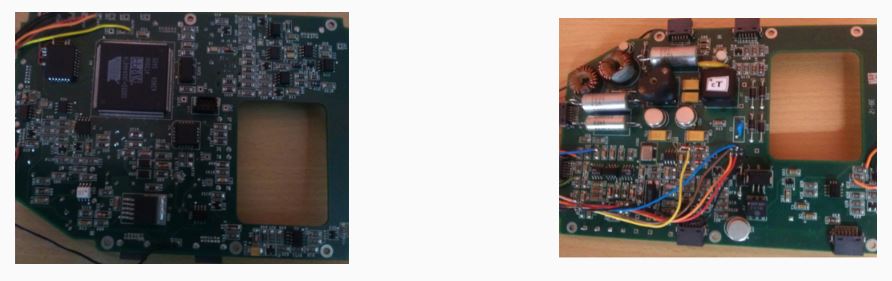
Case Study: Laser Range Finder
The Gunner's Main Sight is now equipped with a laser range finder, thanks
to the re-engineered Controller PCB provided by RTS through Bharat
Electronics Limited for CVRDE.
By updating the outdated board with
modern components, RTS was able to offer a Form, Fit, and Function (F3)
Solution that met all necessary qualifications.