PCB Development

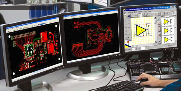
PCB design and analysis are fundamental aspects of creating efficient and reliable electronic devices. The process begins with defining the schematic, where the circuit's functionality is outlined. This schematic is then translated into a PCB layout, which involves placing and routing components on the board to ensure optimal performance and minimal signal interference.
Our HW design full turn-key services include:
- Design idea development, block diagram, power estimate.
- Schematic capture, and BOM cost estimate.
- Enclosure/chassis design.
- PCB floor-plan study.
- PCB Layout Design.
- Thermal/Power Simulation.
- Power Integrity and Signal Integrity Analysis.
- PCB fabrication and assembly.
- Board bring-up and testing.
- HW user manual, and application notes.
PCB Board Design Services:
- System and Board Level Architecture Specification.
- Engineering Design Specification.
- Component Selection.
- Component Obsolescence and Planning.
- Symbol Creation.
- Schematic Drawing/Capture.
- Timing Analysis.
- Netlist Generation.
- BOM Generation.
- Tools: (KiCAD, Eagle, HDL Altium)
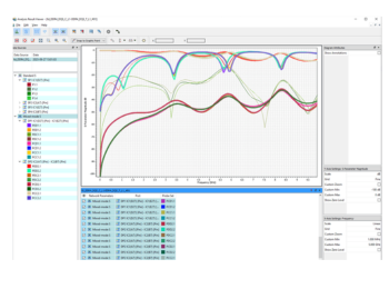
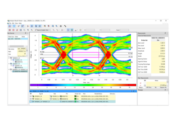
Signal Integrity
RTS with extensive experience in SI, works with you at the beginning of the design to mutually determine the practical level of simulation required for your specific board, to mitigate the risk.
Signal integrity is becoming an increasingly important element of circuit and PCB design. As frequencies used within digital circuits rise, even comparatively short connections act as transmission lines, and they have an effect of the integrity of the signals being carried. These effects can cause circuits not to work, and accordingly, signal integrity is now a major issue for any circuit design.
High-Speed PCB Design Challenges can be overcome through Signal Integrity Analysis and their solutions.
Signal integrity or SI is a set of measures of the quality of an electrical signal. In digital electronics, a stream of binary values is represented by a voltage (or current) waveform.
The simulation software used is Hyper lynx 8.2 update-1. This report is a post-layout analysis report.
Study of Overshoot, Undershoot and Reflections, and Termination analysis
Signal topologies and their analysis.
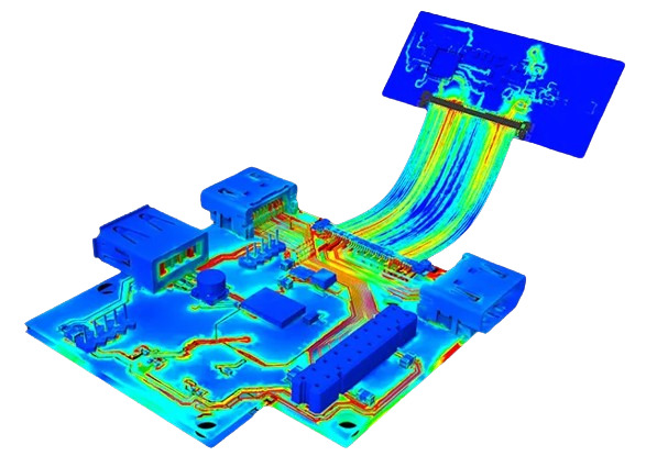
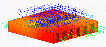
Thermal Analysis
A vital component of PCB design is thermal analysis, which guarantees the board will function dependably in a range of temperatures. A PCB's longevity and performance are ensured by effective thermal management, which also helps minimize overheating and component failure. Key actions and things to keep in mind when doing thermal analysis in PCB design are as follows:
Steps for Thermal Analysis in PCB Design
- Identify Heat Sources
- Determine Thermal Limits
- Create a Thermal Model
- Simulate Heat Distribution
- Optimize Component Placement
- Improve Thermal Dissipation
- Use Thermal Management Components
- Ventilation and Cooling
- Perform Real-World Testing
- Iterate and Refine
Considerations for Thermal Analysis
- Board Material
- Layer Stackup
- Component Derating
- Environmental Factors
Example Tools for Thermal Analysis
- ANSYS Icepak: Specialized in thermal management simulations for electronics.
- Mentor Graphics FloTHERM: Widely used for thermal analysis in electronic design.
- Altium Designer: Includes thermal analysis capabilities within the PCB design environment.
- SolidWorks: Provides thermal analysis as part of its simulation suite.
By incorporating these steps and considerations into your PCB design process, you can ensure that your board operates within safe temperature limits, enhancing the reliability and lifespan of your product.